(Hong Kong)

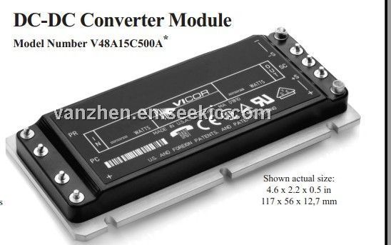
Product Summary
The V48C3V3C75A2 is a DC-DC Converter Module. It uses 2nd Generation power processing, control and packaging technologies to provide the performance, flexibility and cost effectiveness expected of a mature power component. For example, a plated-cavity core transformer couples widely separated primary and secondary windings, resulting in low in-to-out parasitic capacitance and noise. The applications of the V48C3V3C75A2 are telecommunications and distributed power systems.
Parametrics
V48C3V3C75A2 absolute maximum ratings: (1)+In to –In voltage:-0.5 to +75.0 Vdc; (2)+In to –In voltage:100 Vdc ; (3)PC to –In voltage:-0.5 to +7.0 Vdc; (4)PR to –In voltage:-0.5 to +7.0 Vdc; (5)+Out to –Out voltage:-0.5 to +7.0 Vdc; (6)SC to –Out voltage:-0.5 to +1.5 Vdc; (7)Isolation voltage (in to out):3000 Vrms; (8)Isolation voltage (in to base):1550 Vrms; (9)Isolation voltage (out to base):500 Vrms; (10)Storage temperature (C–Grade):-40 to +125℃; (11)Operating temperature (C–Grade):-20 to +100℃; (12)Pin soldering temperature:500℃; (13)Pin soldering temperature:750℃; (14)Mounting torque:5 (0.57) in-lbs (N-m).
Features
V48C3V3C75A2 features: (1)DC input range: 36 to 75V; (2)Input surge withstand: 100V for 100ms; (3)DC output: 5V; (4)Programmable output: 10 to 110%; (5)Regulation: ±0.2% no load to full load; (6)Efficiency: 83%; (7)Maximum operating temperature:100℃ at full load; (8)Power density: 30W/cubic inch; (9)Height above board: 0.43 in. (10,9 mm); (10)Parallelable, with N+M fault tolerance; (11)Low noise ZCS/ZVS architecture.
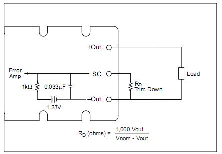
Diagrams