Product Summary
The 74HC4052RM13TR is a dual four-channel analog multiplexer/ demultiplexer fabricated with silicon gate C2MOS technology and it is pin to pin compatible with the equivalent metal gate CMOS4000B series. All inputs are equipped with protection circuits against static discharge and transient excess voltage.
Parametrics
74HC4052RM13TR absolute maximum ratings: (1)VCC, the parameter is supply voltage, the value: -0.5 to +7V; (2)VCC-VEE, the parameter is supply voltage, the value: -0.5 to +13V; (3)VI, the parameter is DC input voltage, the value: -0.5 to VCC + 0.5V; (4)VI/O,the parameter is switch I/O voltage,the value VEE: -0.5 to VCC + 0.5V; (5)ICK, the parameter is control input diode current, the value: ±20mA;(6)IOK, the parameter is I/O diode current, the value: ±20mA;(7)IT, the parameter is switch through current, the value: ±25mA;(8)ICC or IGND, the parameter is DC VCC or ground current, the value: ±50mA;(9)PD, the parameter is power dissipation, the value: 500mW;(10)Tstg, the parameter is storage temperature, the value: -65 to +150℃; (11)TL, the parameter is lead temperature(10 sec), the value: 300℃.
Features
74HC4052RM13TR features: (1)low power dissipation: ICC = 4mA(MAX.) at TA=25℃; (2)logic level translation to enable 5V logic signal to communicate with ±5V analog signal; (3)low on resistance: 70W TYP. (VCC - VEE = 4.5V), 50W TYP. (VCC - VEE = 9V); (4)wide analog input voltage range: ±6V; (5)fast switching: tpd = 15ns (TYP.) at TA = 25 ℃; (6)low crosstalk between switches; (7)high ON/OFF output voltage ratiO; (8)wide operating supply voltage range (VCC - VEE) = 2V to 12V; (9)low sine wave distortion: 0.02% at VCC - VEE = 9V; (10)high noise immunity: VNIH = VNIL = 28 % VCC (MIN.); (11)pin and function compatible with 74 series 4052.
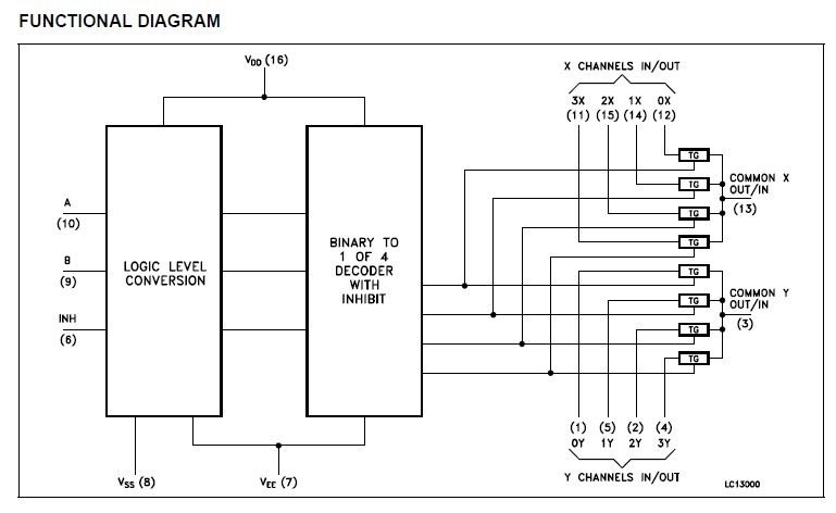
Diagrams

 (Hong Kong)


