 (Hong Kong)

Product Summary
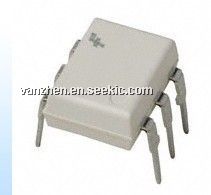
The H11AV2M is a phototransistor optocoupler. The H11AV2M consists of a gallium arsenide infrared emitting diode driving a silicon phototransistor in a 6-pin dual in-line white package. The applications of the H11AV2M include Power supply regulators, Digital logic inputs, Microprocessor inputs.
Parametrics
H11AV2M absolute maximum ratings: (1)Storage Temperature, TSTG: -40 to +150 ℃; (2)Operating Temperature, TOPR: -40 to +100 ℃; (3)Wave solder temperature, TSOL: 260 for 10 sec ℃; (4)Total Device Power Dissipation @ TA = 25 ℃, Derate above 25 ℃, PD: 250 mW, 2.94 mW/℃; (5)DC/Average Forward Input Current, IF: 60 mA; (6)Reverse Input Voltage, VR: 6V; (7)LED Power Dissipation @ TA = 25 ℃, Derate above 25 ℃, PD: 120 mW, 1.41 mW/℃; (8)Collector-Emitter Voltage, VCEO: 70 V; (9)Collector-Base Voltage, VCBO: 70 V; (10)Emitter-Collector Voltage, VECO: 7V; (11)Detector Power Dissipation @ TA = 25 ℃, Derate above 25 ℃, PD: 150 mW, 1.76 mW/℃.
Features
H11AV2M features: (1)H11AV2M feature 0.4” input-output lead spacing; (2)UL recognized; (3)VDE recognized, Add option V.
Diagrams

| Image | Part No | Mfg | Description |  |
Pricing (USD) |
Quantity | ||||
|---|---|---|---|---|---|---|---|---|---|---|
 |
 H11AV2M |
Fairchild Semiconductor |
Transistor Output Optocouplers 0.4" Optocoupler Phototransistor |
Data Sheet |
Negotiable |
|
||||
|
H11AV2M_Q |
Fairchild Semiconductor |
Transistor Output Optocouplers 0.4" Optocoupler Phototransistor |
Data Sheet |
Negotiable |
|
||||