(Hong Kong)

Product Summary
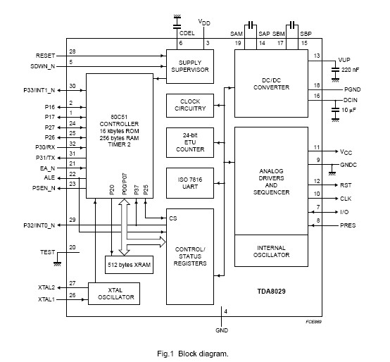
The TDA8029HL/C207 is a complete one chip, low cost, low power, robust smart card reader. Its different power reduction modes and its wide supply voltage range allow its use in portable equipment. Due to specific versatile hardware, a small embedded software program allows the control of most cards available in the market. The control from the host may be done through a standard serial interface. The applications of the TDA8029HL/C207 include Portable card readers, General purpose card readers, EMV compliant card readers.
Parametrics
TDA8029HL/C207 absolute maximum ratings: (1)VDCIN input voltage for the DC/DC converter: -0.5 to +6.5 V; (2)VDD supply voltage: -0.5 to +6.5 V; (3)Vn voltage limit on pins SAM, SBM, SAP, SBP and VUP: -0.5 to 7.5 V; (4)on all other pins: -0.5 to VDD + 0.5 V; (5)Ptot continuous total power dissipation Tamb = -40 to +90℃: 500 mW; (6)Tstg storage temperature: -55 to +150℃; (7)Tj junction temperature: 125℃; (8)Vesd electrostatic discharge voltage human body model; on pins I/O, VCC, RST, CLK and GNDC note 1: -6 to +6 kV; (9)on pin PRES: -3 to +3 kV; (10)on pins SAM and SBM: -1 to +1 kV; (11)on other pins: -2 to +2 kV.
Features
TDA8029HL/C207 features: (1)80C51 core with 16 kbytes ROM, 256 bytes RAM and 512 bytes XRAM; (2)Specific ISO7816 UART, accessible with MOVX instructions for automatic convention processing, variable baud rate, error management at character level for T = 0 and T = 1 protocols, extra guard time, etc.; (3)Specific versatile 24-bit Elementary Time Unit (ETU) counter for timing processing during Answer To Reset (ATR) and for T = 1 protocol; (4)VCC generation (5 V ± 5 % or 3 V ± 5 % or 1.8 V), maximum current 65 mA with controlled rise and fall times; (5)Card clock generation up to 20 MHz with three times synchronous frequency doubling (fXTAL, 1/2fXTAL, 1/4fXTAL and 1/8fXTAL); (6)Card clock stop HIGH or LOW or 1.25 MHz from an integrated oscillator for card power reduction modes; (7)Automatic activation and deactivation sequences through an independant sequencer; (8)1 to 8 characters FIFO in reception mode; (9)Parity error counter in reception mode and in transmission mode with automatic retransmission; (10)Versatile 24-bit time-out counter for ATR and waiting times processing; (11)Specific ETU counter for Block Guard Time (BGT) (22 ETU in T = 1 and 16 ETU in T = 0); (12)Supports synchronous cards which do not use C4/C8; (13)Current limitations on card contacts; (14)Supply supervisor for power-on/off reset and spikes killing; (15)DC/DC converter (supply voltage from 2.7 to 6 V), doubler, tripler or follower according to VCC and VDD; (16)Shut-down input for very low power consumption; (17)Enhanced ESD protection on card contacts (6 kV minimum); (18)Software library for easy integration; (19)Communication with the host through a standard full duplex serial link at programmable baud rates; (20)One external interrupt input and four general purpose I/Os.
Diagrams
| Image | Part No | Mfg | Description |  |
Pricing (USD) |
Quantity | ||||||||||||
|---|---|---|---|---|---|---|---|---|---|---|---|---|---|---|---|---|---|---|
 |
 TDA8029HL/C207,118 |
NXP Semiconductors |
I/O Controller Interface IC SMART CARD READER |
Data Sheet |
|
|
||||||||||||
|
TDA8029HL/C207,151 |
NXP Semiconductors |
I/O Controller Interface IC IOCTRL 5V 0.25A 0.5W |
Data Sheet |
|
|
||||||||||||