(Hong Kong)

Product Summary
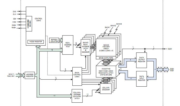
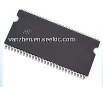
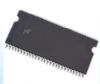
The MT48LC8M16A2P-75IT:G is a high-speed CMOS, dynamic random-access memory containing 134,217,728 bits. The MT48LC8M16A2P-75IT:G is internally configured as a quad-bank DRAM with a synchronous interface (all signals are registered on the positive edge of the clock signal, CLK). Each of the x4’s 33,554,432-bit banks is organized as 4,096 rows by 2,048 columns by 4 bits. Each of the x8’s 33,554,432-bit banks is organized as 4,096 rows by 1,024 columns by 8 bits. Each of the x16’s 33,554,432-bit banks is organized as 4,096 rows by 512 columns by 16 bits. The MT48LC8M16A2P-75IT:G provides for programmable READ or WRITE burst lengths of 1, 2, 4, or 8 locations, or the full page, with a burst terminate option.
Parametrics
MT48LC8M16A2P-75IT:G absolute maximum ratings: (1)Voltage on VDD/VDDQ Supply, Relative to VSS: -1V to +4.6V; (2)Voltage on Inputs, NC or I/O Pins, Relative to VSS: -1V to +4.6V; (3)Operating Temperature, TA: 0 to +70 ℃; (4)Operating Temperature, TA(extended; IT parts): -40 to +85 ℃; (5)Storage Temperature (plastic): -55 to +150 ℃; (6)Power Dissipation: 1W.
Features
MT48LC8M16A2P-75IT:G features: (1)PC100-, and PC133-compliant; (2)Fully synchronous; all signals registered on positive edge of system clock; (3)Internal pipelined operation; column address can be changed every clock cycle; (4)Internal banks for hiding row access/precharge; (5)Programmable burst lengths: 1, 2, 4, 8, or full page; (6)Auto Precharge, includes CONCURRENT AUTO PRECHARGE, and Auto Refresh Modes; (7)Self Refresh Mode; standard and low power; (8)64ms, 4,096-cycle refresh; (9)LVTTL-compatible inputs and outputs; (10)Single +3.3V ±0.3V power supply.
Diagrams