Product Summary
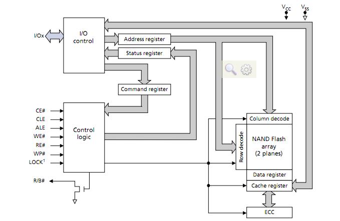
The MT29F1G08ABAEAWP:E is an NAND Flash Memory. The MT29F1G08ABAEAWP:E includes an asynchronous data interface for high-performance I/O operations. The MT29F1G08ABAEAWP:E uses a highly multiplexed 8-bit bus (I/Ox) to transfer commands, address, and data. There are five control signals used to implement the asynchronous data interface: CE#, CLE, ALE, WE#, and RE#. Additional signals control hardware write protection and monitor device status (R/B#).
Parametrics
MT29F1G08ABAEAWP:E absolute maximum ratings: (1)Voltage input, VIN: -0.6 to 2.4 V; (2)VCC supply voltage, VCC: -0.6 to 2.4 V; (3)Storage temperature, TSTG: -65 to +150 ℃; (4)Short circuit output current, I/Os: 5 mA.
Features
MT29F1G08ABAEAWP:E features: (1)Open NAND Flash Interface (ONFI) 1.0-compliant1; (2)Single-level cell (SLC) technology; (3)Organization; (4)Asynchronous I/O performance; (5)Array performance; (6)Command set: ONFI NAND Flash Protocol; (7)Advanced command set; (8)Operation status byte provides software method for detecting; (9)Ready/Busy# (R/B#) signal provides a hardware method of detecting operation completion; (10)WP# signal: Write protect entire device; (11)First block is valid when shipped from factory with ECC. For minimum required ECC, see Error Management.; (12)Block 0 requires 1-bit ECC if PROGRAM/ERASE cycles are less than 1000; (13)RESET (FFh) required as first command after power-on; (14)Alternate method of device initialization after power up; (15)Internal data move operations supported within the plane from which data is read; (16)Quality and reliability; (17)Operating voltage range VCC: 2.7–3.6V; (18)Operating temperature: Commercial: 0 to +70 ℃; (19)Package: 48-pin TSOP type 1, CPL.
Diagrams

 (Hong Kong)


