(Hong Kong)

Product Summary
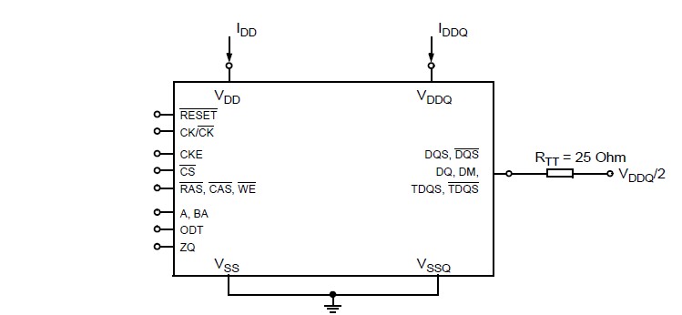
The K4B2G1646E-BCKO is a 2Gb DDR3 SDRAM C-die. It is organized as a 16Mbit x 16 I/Os x 8 banks device. The K4B2G1646E-BCKO achieves high speed double-data-rate transfer rates of up to 2133Mb/sec/pin (DDR3-2133) for general applications. The chip is designed to comply with the following key K4B2G1646E-BCKO features such as posted CAS, Programmable CWL, Internal (Self) Calibration, On Die Termination using ODT pin and Asynchronous Reset.
Parametrics
K4B2G1646E-BCKO absolute maximum ratings: (1)Voltage on VDD pin relative to Vss: -0.4 V ~ 1.975 V; (2)Voltage on VDDQ pin relative to Vss: -0.4 V ~ 1.975 V; (3)Voltage on any pin relative to Vss: -0.4 V ~ 1.975 V; (4)Storage Temperature: -55 to +100 °C.
Features
K4B2G1646E-BCKO features: (1)JEDEC standard 1.5V ± 0.075V Power Supply; (2)VDDQ = 1.5V ± 0.075V; (3)400 MHz fCK for 800Mb/sec/pin, 533MHz fCK for 1066Mb/sec/pin, 667MHz fCK for 1333Mb/sec/pin, 800MHz fCK for 1600Mb/sec/pin, 900MHz fCK for 1866Mb/sec/pin, 1000MHz fCK for 2133Mb/sec/pin; (4)8 Banks; (5)Programmable CAS Latency(posted CAS): 5,6,7,8,9,10,11,13,14; (6)Programmable Additive Latency: 0, CL-2 or CL-1 clock; (7)Programmable CAS Write Latency (CWL)= 5 (DDR3-800), 6 (DDR3-1066), 7 (DDR3-1333), 8 (DDR3-1600), 9(DDR3-1866)and 10(DDR3-2133); (8)8-bit pre-fetch; (9)Burst Length: 8 (Interleave without any limit, sequential with starting address “000” only), 4 with tCCD = 4 which does not allow seamless read or write [either On the fly using A12 or MRS]; (10)Bi-directional Differential Data-Strobe.
Diagrams