Product Summary
The EP2C20F256I8N is an FPGA extending the low-cost FPGA density range to 68,416 logic elements (LEs) and providing up to 622 usable I/O pins and up to 1.1 Mbits of embedded memory. The EP2C20F256I8N is manufactured on 300-mm wafers using TSMC’s 90-nm low-k dielectric process to ensure rapid availability and low cost. By minimizing silicon area, the EP2C20F256I8N can support complex digital systems on a single chip at a cost that rivals that of ASICs. Unlike other FPGA vendors who compromise power consumption and performance for low-cost, the EP2C20F256I8N offers 60% higher performance and half the power consumption of competing 90-nm FPGAs. The low cost and optimized feature set of the device make the EP2C20F256I8N ideal solutions for a wide array of automotive, consumer, communications, video processing, test and measurement, and other end-market solutions.
Parametrics
EP2C20F256I8N absolute maximum ratings: (1)VCCINT, Supply voltage With respect to ground: –0.5 to 1.8 V; (2)VCCIO, Output supply voltage: –0.5 to 4.6 V; (3)VCCA_PLL, PLL supply voltage: –0.5 to 1.8 V; (4)VIN, DC input voltage: –0.5 to 4.6 V; (5)IOUT, DC output current, per pin: –25 to 40 mA; (6)TSTG, Storage temperature No bias: –65 to 150℃; (7)TJ, Junction temperature BGA packages under bias: 125℃.
Features
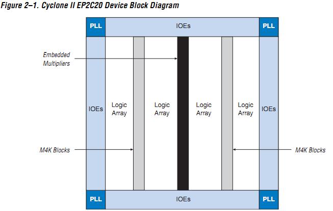
EP2C20F256I8N features: (1)M4K embedded memory blocks; (2)Up to 1.1 Mbits of RAM available without reducing available logic; (3)4,096 memory bits per block (4,608 bits per block including 512 parity bits); (4)Variable port configurations of ×1, ×2, ×4, ×8, ×9, ×16, ×18, ×32, and ×36; (5)True dual-port (one read and one write, two reads, or two writes) operation for ×1, ×2, ×4, ×8, ×9, ×16, and ×18 modes; (6)Byte enables for data input masking during writes; (7)Up to 260-MHz operation; (8)Up to 150 18- × 18-bit multipliers are each configurable as two independent 9- × 9-bit multipliers with up to 250-MHz performance; (9)Optional input and output registers; (10)High-speed differential I/O standard support, including LVDS, RSDS, mini-LVDS, LVPECL, differential HSTL, and differential SSTL ; (11)Single-ended I/O standard support, including 2.5-V and 1.8-V, SSTL class I and II, 1.8-V and 1.5-V HSTL class I and II, 3.3-V PCI and PCI-X 1.0, 3.3-, 2.5-, 1.8-, and 1.5-V LVCMOS, and 3.3-, 2.5-, and 1.8-V LVTTL; (12)Peripheral Component Interconnect Special Interest Group (PCI SIG) PCI Local Bus Specification, Revision 3.0 compliance for 3.3-V operation at 33 or 66 MHz for 32- or 64-bit interfaces; (13)PCI Express with an external TI PHY and an Altera PCI Express ×1 Megacore? function.
Diagrams

| Image | Part No | Mfg | Description |  |
Pricing (USD) |
Quantity | ||||||
|---|---|---|---|---|---|---|---|---|---|---|---|---|
 |
 EP2C20F256I8N |
 |
 IC CYCLONE II FPGA 20K 256-FBGA |
 Data Sheet |

|
|
||||||
| Image | Part No | Mfg | Description |  |
Pricing (USD) |
Quantity | ||||||
 |
 EP2C15AF256C6N |
 |
 IC CYCLONE II FPGA 15K 256-FBGA |
 Data Sheet |

|
|
||||||
 |
 EP2C15AF256C7N |
 |
 IC CYCLONE II FPGA 15K 256-FBGA |
 Data Sheet |

|
|
||||||
 |
 EP2C15AF256C8N |
 |
 IC CYCLONE II FPGA 15K 256-FBGA |
 Data Sheet |

|
|
||||||
 |
 EP2C15AF256I8N |
 |
 IC CYCLONE II FPGA 15K 256-FBGA |
 Data Sheet |

|
|
||||||
 |
 EP2C15AF484C6N |
 |
 IC CYCLONE II FPGA 15K 484-FBGA |
 Data Sheet |

|
|
||||||
 |
 EP2C15AF484C7N |
 |
 IC CYCLONE II FPGA 15K 484-FBGA |
 Data Sheet |

|
|
||||||
 (Hong Kong)


