(Hong Kong)

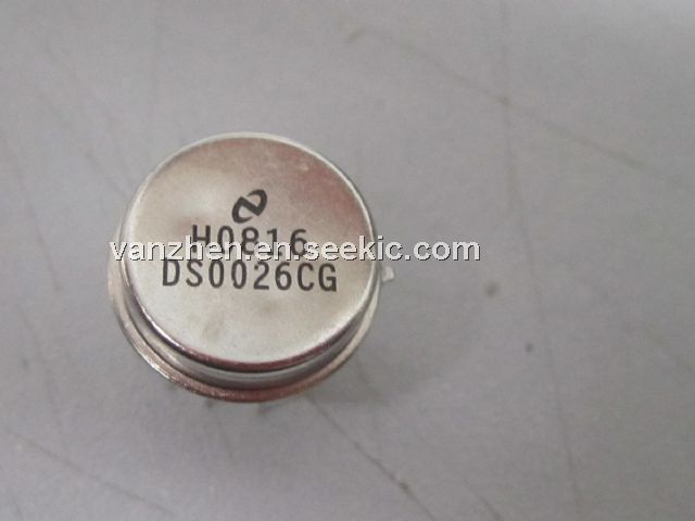
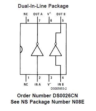
Product Summary
The DS0026CG is a low cost monolithic high speed two phase MOS clock driver and interface circuit. Unique circuit design provides both very high speed operation and the ability to drive large capacitive loads. The device accepts standard TTL outputs and converts them to MOS logic levels. The DS0026CG may be driven from standard 54/74 series and 54S/74S series gates and flip-flops or from drivers such as the DS8830 or DM7440. The DS0026CG is intended for applications in which the output pulse width is logically controlled; i.e., the output pulse width is equal to the input pulse width.
Parametrics
DS0026CG absolute maximum ratings: (1)V+ - V- Differential Voltage: 22V; (2)Input Current: 100 mA; (3)Input Voltage (VIN- V-): 5.5V; (4)Peak Output Current: 1.5A; (5)Maximum Power Dissipation at TA =25℃: 420mW; (6)Operating Temperature Range: 0 to +70℃; (7)Storage Temperature Range: -65 to +150℃; (8)Lead Temperature (Soldering, 10 sec.) 300℃.
Features
DS0026CG features: (1)Fast rise and fall times—20 ns 1000 pF load; (2)High output swing—20V; (3)High output current drive—±1.5 amps; (4)TTL compatible inputs; (5)High rep rate—5 to 10 MHz depending on power dissipation; (6)Low power consumption in MOS “0” state—2 mW; (7)Drives to 0.4V of GND for RAM address drive.
Diagrams