(Hong Kong)

Product Summary
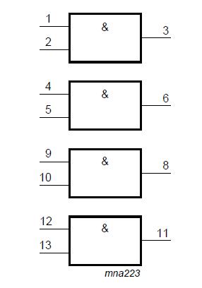
The 74HC08PW is a quad 2-input AND gate. Inputs include clamp diodes. This enables the use of current limiting resistors to interface inputs to voltages in excess of VCC.
Parametrics
74HC08PW absolute maximum ratings: (1)VCC supply voltage: -0.5 to +7 V; (2)IIK input clamping current VI < -0.5 V or VI > VCC + 0.5 V: ±20 mA; (3)IOK output clamping current VO < -0.5 V or VO > VCC + 0.5 V: ±20 mA; (4)IO output current, -0.5 V < VO < VCC + 0.5 V: ±25 mA; (5)ICC supply current: 50 mA; (6)IGND ground current: 50 mA; (7)Tstg storage temperature: -65 to +150℃; (8)Ptot total power dissipation, DIP14 package: 750 mW.
Features
74HC08PW features: (1)Complies with JEDEC standard JESD7A; (2)Complies with JEDEC standard JESD8-1A; (3)Input levels: For 74HC08: CMOS level; For 74HCT08: TTL level; (4)ESD protection: HBM JESD22-A114F exceeds 2000 V; MM JESD22-A115-A exceeds 200 V; (5)Multiple package options; (6)Specified from -40℃ to +85℃ and from -40℃ to +125℃.
Diagrams
| Image | Part No | Mfg | Description |  |
Pricing (USD) |
Quantity | ||||||||||||
|---|---|---|---|---|---|---|---|---|---|---|---|---|---|---|---|---|---|---|
 |
 74HC08PW,112 |
NXP Semiconductors |
Gates (AND / NAND / OR / NOR) QUAD 2-INPUT AND |
Data Sheet |
|
|
||||||||||||
|
74HC08PW,118 |
NXP Semiconductors |
Gates (AND / NAND / OR / NOR) QUAD 2-INPUT AND |
Data Sheet |
|
|
||||||||||||