Product Summary
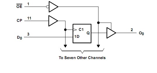
The 74FCT374ATSO is a high-speed, low-power, octal D-type flip-flop, featuring separate D-type inputs for each flip-flop. The 74FCT374ATSO has 3-state outputs for bus-oriented applications. A buffered clock (CP) and output-enable (OE) inputs are common to all flip-flops. The eight flip-flops in the 74FCT374ATSO store the state of their individual D inputs that meet the setup-time and hold-time requirements on the low-to-high CP transition. When OE is low, the contents of the eight flip-flops are available at the outputs. When OE is high, the outputs are in the high-impedance state. The state of OE does not affect the state of the flip-flops.
Parametrics
74FCT374ATSO absolute maximum ratings: (1)Supply voltage range to ground potential:–0.5 V to 7 V; (2)DC input voltage range: –0.5 V to 7 V; (3)DC output voltage range: –0.5 V to 7 V ; (4)DC output current (maximum sink current/pin): 120mA; (5)Package thermal impedance, θJA (see Note 1): P package: 69℃/W; (6)Q package: 68℃/W; (7)SO package: 58℃/W; (8)Ambient temperature range with power applied, TA –65 to 135℃; (9)Storage temperature range, Tstg –65 to 150℃.
Features
74FCT374ATSO features: (1)Function, Pinout, and Drive Compatible With FCT and F Logic; (2)Reduced VOH (Typically = 3.3 V) Versions of Equivalent FCT Functions; (3)Edge-Rate Control Circuitry for Significantly Improved Noise Characteristics; (4)Ioff Supports Partial-Power-Down Mode Operation; (5)Matched Rise and Fall Times; (6)Fully Compatible With TTL Input and Output Logic Levels; (7)ESD Protection Exceeds JESD 22; (8)Edge-Triggered D-Type Inputs; (9)250-MHz Typical Switching Rate; (10)3-State outputs.
Diagrams

| Image | Part No | Mfg | Description |  |
Pricing (USD) |
Quantity | ||||
|---|---|---|---|---|---|---|---|---|---|---|
 |
 74FCT374ATSOG |
 Other |
 |
 Data Sheet |
 Negotiable |
|
||||
 |
 74FCT374ATSOG8 |
 Other |
 |
 Data Sheet |
 Negotiable |
|
||||
 (Hong Kong)


